本文最后更新于:2024年5月7日 下午
本文记录芯片制造中的掩模部分术语。
A
| 名词 | 解释 |
|---|---|
| AAPSM/Levenson | Alternating Aperture Phase Shift Mask (see also Levenson) an etched quartz reticle which incorporates a light blocking layer of chrome or moly silicide coupled with etched quartz trenches, to create alternating 0? and 180? angles. |
| Address (or Address Unit) | The size of the grid on which a mask pattern is designed. |
| Alias | An accepted abbreviation of specified customer names. For instance, Texas Intruments = TI. |
| Alpha Corrections | Corrections for X and Y scaling and orthogonality in the jobdeck. |
| ALT | A lithography system that uses a laser to expose the resist on a photomask blank. |
| ALTA 3000 | A fourth generation laser tool featuring a 20X reduction lens and a 8.33 nanometer writing grid. |
| ALTA 3500 | A fifth generation laser tool featuring a 33X reduction lens and a 5 nanometer writing grid. |
| AMS - 100/200 | A line width measurement system with a manual stage. |
| Angstrom | A metric unit of measure equal to 1/10000th of a micron, most often used to express thickness |
| Anodized | A special layer of metal coating on a mask. |
| Anomaly | An atypical defect or problem with a mask. |
| Anti-Scattering Bar | An optical proximity correction reticle feature routinely used by customers that utilize MicroUnity software to generate reticle pattern data. |
| APA Algorithm | A software enhancement for KLA 351 systems that aids in the die-to-database inspection of OPC enhanced and Phase Shift reticles. |
| Applications Engineer | Appl eng is an abbreviation for application engineer. |
| AR | Abbreviation for anti-reflective coating. |
| Array | The arrangement of rows and columns of die on a photomask. Artifact |
| ASIC | Abbreviation for Application Specific Integrated Circuit which is a chip designed for a specific end user with a unique purpose. |
| AESOP | Automated Electron Source Optics Program is the automatic setup function of the column on e-beam lithography systems. |
| ASSP | Abbreviation for Application Specific Standard Product which is a chip designed for a unique purpose that can be sold to a broad range ofend users. |
| Assist Features | Reticle features intended to improve lithography on a customer wafer. (see also OPC, serifs, hammerheads, scattering bars and anti-scattering bars) |
| Assist Slots | A specific assist feature intended to improve resolution on contacts. (see also assist features) |
| Auxiliary Pattern | A pattern containing no circuitry thatsurrounds a smaller pattern in order toclear out a specified window area and isolate the smaller pattern |
B
| 名词 | 解释 |
|---|---|
| Best Fit | The point at which the maximum positional error between a mask and a reference registration grid is minimized through best-fit alignment. |
| Binary Mask or Reticle | A mask or reticle that has chrome on quartz without etched trenches. |
| Blank Material | The glass used to make a photomask. It is coated with chrome, antireflective coating, and photoresist. |
| Blank Pattern | A pattern containing no circuitry which is used to clear a specified window area. |
| Boolean Derivation | A logical means of deriving photomask layer pattern data from other layers of the mask set. |
| Bumping | 植球,是一种在晶圆上形成微小的焊球或铜柱的制造工艺。 |
C
| 名词 | 解释 |
|---|---|
| Capture Rate | The percentage rate at which a defect inspection tool can find defects of a given size, for example 99.5% of .25 micron defects (also called sensitivity) |
| CATS | Computer Aided Transcription Software is the primary fracturing and data viewing software used at all Photronics facilities. This software, developed by Transcription Enterprises, has the ability to simulate complete jobdeck (mask layout) schemes for the purposes of viewing the data prior to the manufacturing process. It is widely used by our customers for a variety of design checks. |
| CD | see Critical Dimension |
| CD Bias | The original and final CD values do not match, thus requiring process manipulation to achieve. see CD Process Push |
| CD Linearity | The degree to which a small feature deviates from its intended size as compared to a larger feature’s deviation on the same mask. |
| CD Mean to Target | The difference between an average (mean) of a given set of CD readings from the actual targeted value. |
| CD Nominal | Customer provided specifications to monitor the size of the geometry within a pattern. |
| CD Process Push | The ability to move a CD value from its written dimension by manipulating the amount of develop time applied at the process stage. |
| CD Range | The difference between the lowest and highest CD values within a given set of readings. |
| CD Tolerance | A plus/minus value that dictates the allowable disparity between each actual CD reading and a target value. The target value may be either an absolute or mean number. |
| CD Uniformity | A specified )often plus/minus) value that dictates the allowable difference between the lowest and highest CD values within a given set of readings. It can apply to either a mean or absolute value. |
| Cell | A design element in a hierarchical database. |
| Cellulose Acetate Nitrocellulose | An organic material used as a pellicle membrane. |
| Centrality | The degree to which a mask pattern or pellicle is centered on a plate. |
| Character Rotation | Allows you to specify the degree that the characters of the mask title have to be rotated for the appropriate appearance. |
| Chip | see Die |
| Chip Check | see Die-to-Database Inspection |
| Chrome | The shiny metallic material that is used as a light blocker on most masks. |
| Chrome Extension | A chrome defect that extends from an intended chrome edge. |
| Chrome Spot | A chrome defect that is isolated from any other chrome. |
| CIF | An abbreviation for Caltech Intermediate Format, hierarchical pattern data format that is used for mask layout. This software is “public domain” meaning available for free without licensing fees. |
| Clamp Interference | The interference caused by placement of mask pattern data at or very near to the clamps on a MEBES substrate cassette or holder. |
| Classify | see Defect Types |
| Clear | An area on the mask where the chrome has been removed and there is only glass. |
| Clear Extension | A clear defect that extends into a chrome area from an intended clear feature. |
| Clear Field | The background area surrounding the component geometry is clear, that is, there is no chrome. |
| Code Layer | A layer or layers used to customize a base array of components. see Gate Array |
| Clock Start Date/Time | The date and time which Photronics Inc. receives all of the required data from the customer. |
| Closure Check | Internal patterns written onto every mask used to monitor the accuracy of the lithography equipment. Half of each pattern is written at the beginning of the write process and half is written at the end. |
| CMOS | Abbreviation for complementary metal oxide semiconductor, a common IC process. |
| C of C | Abbreviation for Certificate of Conformance, a quality document that list the inspections required, the pass fail criteria and the results for a specific mask. |
| Comp O | Comp O (ortho) controls the squareness of the patterns in the reticles. |
| Comp X | Comp X controls the height of the pattern along the X axis. |
| Comp Y | Comp Y controls the width of the pattern along the Y axis. |
| Compact | A container in which a photomask is stored. Compacts come in a wide variety of sizes and colors to accommodate different mask and pellicle sizes. |
| Compaction | A process by which a large data file containing highly repetitive structures can be reduced in file size. |
| Contamination | Particles, dirt or haze on a photomask. |
| Contract Date/Time | The date and time the finished product is quoted to be shipped to the customer. This is not a quoted receipt date of the product. |
| CORE | A lithography systems that use a laser to expose the resist on a photomask blank, stands for Customer Optical Reticle Engraver, various Core models include 2000, 2100, 2100XP, 2500, 2564. |
| Corner Rounding | The degree to which feature corners that should be at sharp angles are rounded by the lithography develop and etch processes. |
| Correlated Nominal | The correlation of the customer CD nominal with the difference between Photronics Inc. and the customer CD nominal calibration standards. |
| Correlation | The delta determined from a correlation exercise, most often refers to critical dimensions. |
| Correlation Exercise | A process by which the results from two different measurement tools are compared to each other based upon readings from a common artifact. |
| Cosmetic Grade | The tolerance for defect that may not affect the circuit geometry. These defects include scratches on the chrome outside of the array, damaged or partially removed AR, or glass chips on the edges of the reticle. |
| Critical Dimension | A geometry or space used as a gauge to monitor the pattern size and ensure that it is within the customer’s specification |
| Cycletime | The cumulative time from receipt of an order to completion. |
D
| 名词 | 解释 |
|---|---|
| Dark Field | The background area surrounding the component geometry is chrome (dark). |
| Data Bias | A predetermined amount of data sizing applied prior to lithography that enables more latitude when processing a mask. This bias facilitates the natural process movement of clear and dark features. |
| Data Express | A software option available on some Orbot systems that enhances the systems ability to inspect very dense and OPC enhanced patterns. |
| Data Extent | The data extent provides data area parameters along the X & Y points. |
| Data Verification/Inspection | see Die-to-Database Inspection |
| Deep UV | Deep Ultraviolet, commonly refers to wave lengths at 248nm, but also applies to 193nm |
| Defect | A flaw affecting the geometry such as unwanted chrome, missing chrome, and dirt. |
| Defect Inspection | An inspection for defects using die to die, die to database or visual methods. |
| Dense/Isolated Bias | Refers to the degree to which the mean of measured dense features differs from the mean of like sized measured isolated features. |
| Density | 1. The relative degree of pattern to no patterned area on a photomask as in circuit density 2. The allowable number of defects at a given size as in defect density |
| Descum | A plasma process after develop and prior to etch where residual surface contaminants are removed. |
| Design Grid | The measurement unit on which all 0 and 90 degree edges of a circuit design fall. |
| Design Rule | The rules applied to circuit designs for a given process a given circuit design size, for example .35micron CMOS design rules. |
| Develop | To treat a mask with chemicals to remove exposed photoresist. This step is part of the write process. |
| Device | The part number/name assigned by the designer to identify the integrated circuit. |
| Die | A single complete integrated circuit device image. |
| Die Size | The physical area a chip takes up on the wafer at 1X. Usually expressed in x-axis by y-axis in microns. |
| Die-to-Die Inspection | An automated defect inspection in which the equipment compares two identical images on the mask having the same pattern and identifies any discrepancies between the two. |
| Die-to-Database Inspection | An automated inspection for data discrepancies. The equipment compares the image on the mask to a database image and identifies any discrepancies between the two. |
| Digitized Data | Data, which has been transformed from geometrical, shapes (patterns) into the computer language of digits. The write tools require this form of data in order to write the mask. |
| DNIR | Abbreviation for Do Not Inspect Region, an area of a mask that can be specified as not to be inspected for defects. |
| DRAM | Abbreviation for Dynamic Random Access Memory, a type of memory chip. |
| Drop-ins | Mask patterns that are placed into an array. |
| DRS I | A laser repair tool manufactured by Quantronix that removes chrome defects. |
| DRS II | A laser repair tool manufactured by Quantronix that removes chrome defects and can fill clear defects with a chrome/molydenum alloy. |
| Dry Etch | The removal of material from a substrate by using a gases in a plasma. |
- Defects
| Defect Types 缺陷类型 | 含义 |
|---|---|
| Bridging | an opaque or clear defect that joins two or more lines of the same type |
| Edge | an opaque or clear defect that joins a feature edge |
| False | a detection by the inspection system that is not a hard defect |
| Glass Damage | damage in the substrate from laser or FIB repair |
| Hard | a defect that is either unintended opaque or unintended clear |
| Isolated | a defect that is not attached to any intended feature |
| Nuisance | a false defect that is routinely detected by the inspection system |
| Soft | a defect that can be subsequently removed from the mask by cleaning processes |
E
| 名词 | 解释 |
|---|---|
| EAPSM | see Embedded Attenuated Phase Shift Mask |
| Ebeam | A lithography system, which uses an electron beam (ebeam) to expose the photoresist on a photomask blank. |
| EBES | The precursor of MEBES systems invented by Bell Labs, Electron Beam Engraving System. |
| EBR-9 | An electron beam sensitive resist used in mask manufacturing. |
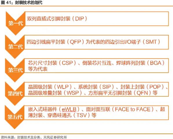
| eWLB | 是一种扇出型晶圆级封装(Fan-out Wafer-Level Package 缩写FO-WLP)技术,将芯片重新布置到一块人工晶圆上,然后向芯片四周扇出重布线、植球、然后进行封装。根据封装技术的划代,eWLB 属于第五代封装技术,是目前最先进的封装技术之一。 |
| Embedded Attenuated Phase Shift Mask | A phase shift mask that achieves the 180 degree attenuation through the properties of the blank coating rather than the etching of quartz. |
| Entry Priority | The entry priority allows the user to indicate the priority of a given job numerically compared to other entered jobs. |
| ESD | see Static Erosion |
| Etch | A process to remove unwanted chrome. In the write process, removing the chrome and AR in the areas where the exposed resist was removed during development. |
| EWT | Estimated write time. An agreed upon limit in minutes for the writing process of the product. |
| EWT Rate | A specified rate for writing time per minute over the estimated write time. |
| EWT Limit | The highest additional amount that can be charged for additional write time beyond the agreed write time. |
| Extent | The extreme edges of a mask pattern as defined by the fracture window. |
F
| 名词 | 解释 |
|---|---|
| False Call | see False Defects |
| False Defects | Defects that are captured by a defect detection system that do not affect the performance of the mask or reticle. |
| Features | see Geometry |
| FIB | see Focused Ion Beam |
| Fiducials | Marks, usually located outside of the array, used to align different layers to one another during wafer fabrication. Each brand and model of stepper have specific types and placements of fiducials. A.k.a. |
| Field UT1X Reticles | Blocks of dice arranged in horizontal rows on the mask. Each field can contain a different device or layer. |
| Field Tone | The appearance (dark or clear) of the background area surrounding the component geometry. |
| Flat | The flat edge of a silicon wafer. |
| Flatness | The peak to valley measure of deviation of a substrate from true planarity. |
| Flat Panel Display | A niche market technology that uses photomasks. |
| Focused Ion Beam | An advanced technology that is used to repair defects on photomasks. |
| Footprint | 1. The residual positional inaccuracy of a mask lithography tool related to the uniqueness of the state mirrors. 2. The physical space a piece of equipment takes up in a clean room. |
| Fracture | The process by which hierarchical mask data is converted to lithography system useable formats. |
| Frame | The patterned area of a reticle that surrounds the individual chips and forms the scribe lines between them. |
| Frame Generation | A process by which the scribe and test structures for reticle are automatically or manually generated. |
| Fringe | The area of a resisted blank near the edge where the resist thickness increases enough to show a visible change in color. |
| FTP | Abbreviation for File Transfer Protocol, a means of sending data files over a computer network such as the internet. |
G
| 名词 | 解释 |
|---|---|
| Gate Array | A circuit design that can be customized for many uses depending on how the device components are connected to each other. A gate array mask set usually uses metal and via layers to customize an existing base set. Also referred to as Codes. |
| GDSII | A common format for hierarchical design that can be easily converted into mask making formats. |
| Geometry | Intended pattern imaged on the photomask. |
| Grating | A mask pattern of lines and spaces covering relatively large areas. |
| Grid | The measurement unit on which all 0 and 90 degree edges of a circuit design fall. |
| Guides | A metal device attached to UT1X reticles for loading onto an Ultratech Stepper. There are two types of guides, wide field and standard field. Wide field guides are attached to the bottom of the reticle. Standard field guides are attached to the sides of the reticle next to the pellicle. |
H
| 名词 | 解释 |
|---|---|
| Halftone Mask | see Embedded Attenuated Phase Shift Mask |
| Hamatech | see Steag |
| Hammerhead | An OPC structure used to reduce corner rounding and line shortening. |
| Hard Align | A registration measurement where one point is chosen for alignment and the deviation of all measured points is referenced to that point. This is the most difficult registration measurement method. |
| Hierarchical | A method of storing pattern by which highly repetitive patterns are represented by a single instance of that pattern cell and the reference coordinates of each cell into a higher level structure. There can be many layers of cells nested inside a top level structure. |
I
| 名词 | 解释 |
|---|---|
| IC | see Integrated Circuit |
| Intergrated Circuit | A fabricated semiconductor manufactured to perform a specific function, is composed of many functional parts such as transistors, resistors and capacitors, etc. Abbreviated |
| International Grid | A distance measurement standard. |
| IPRO | see LMS |
J
| 名词 | 解释 |
|---|---|
| JCL | Acronym for Job Control File, the file created by post processing MEBES job decks and pattern files on an Etec CORE or ALTA tool used by the CORE & ALTA tools as a jobdeck is used by the MEBES tools. |
| Jobdeck | The instruction for placement of all the different patterns on a mask. |
| Job View | An approval point in the mask making process, after completion of the jobdeck and prior to committing to write. |
| Justification | The alignment of mask titles in a job deck as in right, left or center justified. |
K
| 名词 | 解释 |
|---|---|
| KLA | A company that manufactures defect inspections systems (now called KLA-Tencor) KLA defect inspection has become synonymous with die to die inspection. |
| KLA Reference Mark | A mark placed in the four corners of the mask used as a point of reference for defect inspection and repair. |
| KLARIS | Abbreviation for KLA Reticle Inspection system, KLARIS defect inspection is synonymous with die to data inspection. |
| KLARIS Tape | Magnetic tape containing fractured data used in a die-to-database inspection on either KLA or KLARIS inspection equipment. |
| KMS | A series of automated programmable line width measurement tools manufactured by Technical Instruments Corporation, with various model names and numbers; KMS300, KMS310, KMS400. |
L
| 名词 | 解释 |
|---|---|
| Layer | One of a series of overlaying photomasks or photomask images, which make up a device. |
| Leica | A German manufacturer and distributor of measurement and lithography tools. |
| Levenson PSM | A phase shift mask with a highly repetitive pattern where every other feature incorporates a 180 degree phase shift. |
| Linearity | The degree to which the relative sizes of large, small, clear and dark features deviate from their intended size. |
| Lithography | Exposure and processing to engrave circuit images onto a photomask blank. Synonymous with write. |
| Abbreviated | Litho |
| LMS | A series of laser interferometer registration measurement tools manufactured by Leica Corp., with various model names and numbers LSM2000, LMS2020, LMS I-Pro. |
| LWD | Abbreviation for Long Working Distance, used to describe the allowable space between a microscope or defect inspection system lens objective and a photomask. LWD objectives are used to inspect and/or measure photomasks with pellicles. |
| LWM200 | An automated programmable high precision line width measurement system manufactured by Leica Corp. |
M
| 名词 | 解释 |
|---|---|
| Manual Inspection | see Visual Inspection |
| Mask | see Photomask |
| Measure File | The coded instruction set for performing measurements on a Nikon or an LMS metrology system. |
| MEBES | Abbreviation for Manufacturing Electron Beam Engraving System, a term used synonymously with ETEC ebeam systems. |
| Micro Inch | A unit of measure equal to 1/1000 of an inch. 1 micro inch = 2.54 microns. |
| MicroLine | A line width measurement microscope |
| Micron | A unit of measure equal to 1/1,000,000th of a meter, about 1000 times thinner than a human hair. |
| Microprocressors | Semiconductor devices that do most of the computations on a computer system. |
| Millimeter | A unit of measure equal to 1/1000th of a meter. |
| Mirror | Inversion of a mask image such that left becomes right and right becomes left. |
| MOF | Abbreviation of Mask Order Form, also used to identify a computer based mask technical specification input program used by some Photronics sites. |
| Monitor Mask | A mask that is written or measured periodically as a means of monitoring the performance of equipment and processes. |
N
| 名词 | 解释 |
|---|---|
| NBS | see NIST |
| Nikon 2I | A laser interferometer-based position and registration measurement tool first introduced in mask shops in the early 1980’s. |
| Nikon 3I | The successor to the Nikon 2I - introduced in the mid 1980’s. |
| Nikon Marks | see Registration Marks |
| NIST | Abbreviation for National Institute of Standards and Technology (formerly NBS, National Bureau of Standards), this agency is tasked with developing and providing standards for industry. |
| Nitrocellulose | An organic material used as a pellicle membrane. |
| Non-mask Items | An item other than a mask item such as data, inspections, specs, pellicles, compacts, etc. |
| Number of Good Fields | The acceptable minimum number of good fields on an UT1X reticle as specified by the customer. |
| Number of Mask Line Items | The number of plates required for the completion of the job. |
O
| 名词 | 解释 |
|---|---|
| OAT | Abbreviation for Optical Alignment Target, a pattern used on Ultratech Reticles for coarse alignment on the wafer. |
| OPC | Abbreviation for Optical Proximity Correction, a reticle enhancement approach where sub-resolution structures are added to circuit designs and imaged on reticles to correct for critical dimension and resolution variations that appear on wafers. |
| Orbot | Trade name for a die to database defect inspection system now manufactured by Applied Materials. |
| Orientation | The relationship of the mask pattern to the original drawn pattern when looking through the mask substrate at the opaque layer. It may be correct (looks the same) or it may be |
| mirrored (looks like the mirror image of the drawing). | |
| Ortho | A job deck command that instructs the lithography tool to match the orthogonality characteristics of a reference artifact. |
| OSI | Abbreviation for Optical Specialties, Inc., a manufacturer of line width measurement microscopes. |
P
| 名词 | 解释 |
|---|---|
| Parity | Whether an image is right reading or wrong reading (mirror image). |
| Particles | Any element of dust or debris on a photomask. |
| Patterns | Features that are imaged on the mask. |
| Pattern Offset | Used when the pattern is not centered on the mask. |
| PBS | see Poly Butene (1) Sulfone |
| PEC | Abbreviation for proximity effect correction, a software enhancement available on advanced lithography systems that adjusts exposure dose to correct for proximity effects. |
| Pellicle | A metal frame over which a thin, transparent film (membrane) is stretched. A pellicle is attached to the photomask over the array or row. Pellicles come in many shapes and sizes to accommodate the different array shapes and sizes of photomasks. They also come with different film types to meet the stepper exposure requirements. The pellicle film keeps the contamination out of the focal plane of the wafer stepper so it will not image onto the wafer. |
| Performance to Schedule (PTS) | Measure of cycle time performance, usually expressed as the percentage of plates shipped on time compared with total plates shipped. |
| Phase Shift Mask (PSM) | A mask that, in addition to blocking light, selectively alters the phase of the light transmitted through the mask to improve depth of focus and resolution on a wafer. |
| Photomask | A glass substrate with a layer of chrome on one side into which a portion of an electronic circuit design is etched. Synonymous with mask and plate. |
| Pinhole | An unintended clear hole in the blank coating material. |
| Plate | see Photomask |
| PNF | Abbreviation for Problem Notification Form, ;an internal document identifying technical issues with a particular mask order. |
| PO | Abbreviation for Purchase Order, the customer’s document specifying order details. |
| Polarity | The tone of the field, either clear or dark. |
| Poly Butene (1) Sulfone (PBS) | A solvent based wet etchable resist that is sensitive to relative low electron beam exposure. |
| Post Pellicle Inspection | A die-to-die or a die-to-database inspection performed after a pellicle has been attached to the mask. A.k.a. |
| Primary | (Pattern and/or Die) The design that will be used to make the main circuit. |
| Print AU | see Scaled Write Address |
| Process | The steps (develop, etch, strip) following the exposure of the image onto the mask. |
| Process Delta | The difference between the data CD size and the CD size on the mask. |
| Proximity Error | An error in feature placement or fidelity related to the back scattering of electrons or photons from exposure nearby features. Also know as proximity effect. |
| PSM | see Phase Shift Mask |
| PTC | Premium time charge. Allows you to specify the number of hours required to qualify for the increased rate, the fewer the hours, the greater the rate. |
| PTC Rate | Premium time charge rate. Allows you to specify the percentage added to the total price for the accelerated manufacturing time. |
Q
| 名词 | 解释 |
|---|---|
| QA | An abbreviation for quality assurance. |
| QC Optics | A surface laser scanning system that scans masks for particles and contamination. |
| Qualification | A series of performance tests specified by the customer prior to a commitment to routine production. |
| Qual Order | Qual order field allows the user to indicate if the job is a qualification job as specified by the customer. |
| Quantronics | A manufacturer of laser based repair systems. |
| Quote | The document generated by sales that communicates prices, agreed upon specifications and cycle times to our customers. |
R
| 名词 | 解释 |
|---|---|
| Race Track | The series of crosses and alignment marks that surround the grouping of fields on an Ultratech 1X reticle. |
| Raster-scan | A writing methodology employed by some ebeam and laser systems whereby the entire mask is addressed in pixelized fashion, and the beam blanks on and off where needed. |
| RDL | 向芯片四周扇出重布线 |
| Receipt Date/Time | The date and time which Photronics Inc. received notification of an upcoming job from the customer. |
| Reflected Light | Refers to taking some kind of reading on a mask (line width, defect inspection, etc.) where the measurement is taken with the light source reflecting off of the surface of the mask. |
| Registration | The positioning of patterns on a layer to corresponding patterns on other layers within the same device or to a design grid. Synonymous with metrology. |
| Registration Marks | Marks put into customer chip or frame data to aide in measuring on a laser interferometer registration tool. Usually these are “L” bars or crosses. |
| Repair | To remove any unintended opaque regions or to make opaque any unintended clear region on a photomask. Usually accomplished with laser or focused ion beam tool. |
| Repeat Count | The repeat exposure of a pattern on a MEBES tool used to increase the exposure energy delivered during write. |
| Resist | A thin photo sensitive or electron sensitive material used both in the manufacturing of photomasks and wafer fabrication for exposing design images onto a substrate. Synonymous with photoresist. |
| Reticle | A photomask with patterns that are stepped (repeated side by side) onto the wafer. |
| Retrace | An option by which an ebeam lithography tool can rewrite over the same feature in order to increase the exposure dose in the resist. Most often used for submicron features. see Repeat Count |
| Reverse Tone | A process by which the polarity of a mask pattern is inverted such that chrome becomes clear and clear becomes chrome. Usually done through the job deck or off line on data processing software. |
| Right Reading | see Parity |
| RMA | Return Material Authorization. All returns and customer complaints relating to product and its shipments are handled by the RMA system that includes a specified form and computer software for documentation. |
S
| 名词 | 解释 |
|---|---|
| Scale Factor | Used to increase or decrease the pattern size. |
| Scaled Write Address | The actual size of the address unit after scaling has been applied. |
| Scaling | Global reduction in chip size, also know as shrinking. |
| Scalpel | Acronym for Scattering with Angular Limitation in Projection Electron-beam Lithography. This is an advanced wafer lithography technology using a strutted membrane mask. |
| SCAR | Abbreviation for Supplier Corrective Action Request. |
| Scattering Bars | An optical proximity correction reticle feature routinely used by customers that utilize MicroUnity software to generate reticle pattern data. |
| SEIKO 1000/3000 | A focused ion beam photomask repair took, the 1000 is the earliest model, the 3000 is the most recent. |
| SEM | Abbreviation for scanning electron microscope. |
| Semiconductor | A material that can either conduct or not conduct electricity depending on what elements or compounds are added to it. |
| Sensitivity | see Capture Rate |
| Serifs | Small features that are added to the corner of mask patterns to reduce corner rounding on wafers. |
| Shrinking | see Scaling |
| Sizing | The increasing or decreasing of line width without scaling through use of software. |
| Snapping | Moving of a feature edge during data fracturing or writing. Caused by the feature edges in the source file not being on an integer of the address unit to which the pattern data is being fractured. |
| Soft Defect | A particle or contaminant on a mask or reticle. |
| Standard Field | A UT1X reticle typically having 4 fields per row (used by the first generation of systems manufactured by Ultratech.) |
| Standard Field Guides | see Guides |
| Static Erosion | Pattern damage on mask chrome feature edges and corners caused by static electricity, also as ESD (electro-static discharge) damage. |
| STARlight | A mask inspection system manufactured by KLA-Tencor that inspects for surface anomalies on a mask by using Simultaneous Transmitted And Reflected light. |
| Steag | A manufacturer of wet chemical processing and cleaning equipment used in photomask manufacturing. |
| Step | The projection of die images onto a wafer side by side to complete an array. |
| Step and Repeat | (Stepping) The repetitive exposing of a single image in different specified places on the wafer. |
| Stepping | see Step and Repeat |
| Stepping Distance | The distance between exposures of pattern in the X and Y axis on a mask. |
| Submicron | Dimensions smaller than 1.0 micron in size. |
| Substrate | The under-laying material. For a mask, substrate refers to a photomask blank. For an IC, it refers to a silicon wafer. |
T
| 名词 | 解释 |
|---|---|
| TAR | Abbreviation for Technical Action Request. |
| Test | (Test Pattern) Simplified functional device (of the same process type as the primary die) used for process control and monitoring during wafer fabrication and sometimes to test new design ideas. |
| Thin Film Head | A magnetic device that reads and/or writes data to a hard disk. |
| Through Pellicle | see Post Pellicle Inspection |
| Thru-pell | see Post Pellicle Inspection |
| Transcription | Refers to Transcription Enterprises, a software company that developed and sells CATS software. |
| Transmitted Light | Refers to taking some kind of reading on a mask (line width, defect inspection, etc.) where the measurement is taken with the light source shining through the mask. |
| Turn Hours | Turn hours is the amount of time (in hours) that Photronics Inc. has to manufacture a mask from the Clock Start Date/Time to the promised shipping date. |
| TPP | Abbreviation for Technical Plan Proposal, which is a document that defines the scope and metrics of a technology development project. |
| Two Point Match | A method of alignment of mask registration data where two arbitrary points (usually fiducials) are selected and aligned to the reference grid, and all other points are compared to the grid based on that alignment. |
U
| 名词 | 解释 |
|---|---|
| Ultrabeam | A division of Ultratech Stepper Corporation that manufactures the V2000 vector-raster ebeam writing system. |
| Ultratech 1X Reticle | A reticle is used by an Ultratech Stepper. Usually composed of 2-6 small fields of mask pattern data, these reticles are made at the same magnification as the end users’ wafers (1X). |
| UT1X Reticle | see Ultratech 1X Reticle |
V
| 名词 | 解释 |
|---|---|
| V2000 | An advanced Vector Raster E-beam system manufactured by Ultabeam Corporation. |
| Vector Raster | A writing methodology employed by some ebeam systems whereby the stage travels to the area of the mask that needs to be exposed and the pattern is written using rasterized data. |
| Vector-scan | A writing methodology employed by some ebeam systems whereby the stage travels to only those areas on a mask that need to be exposed rather than scanning the entire mask surface. |
| Virtual Address | A software enhancement for MEBES ebeam write tools that allows the tool to approximate line edges by doubling the address unit and exposing every other pixel. This feature is usually used to speed up write times on mask patterns with small address units where edge roughness is not a concern. |
| Visual Inspection | Inspection for defects done using a non-automated microscope or the unaided eye. |
W
| 名词 | 解释 |
|---|---|
| Wafer | A thin slice of silicon, the substrate used in producing integrated circuits. |
| Wafer Fab | The clean-room manufacturing area where wafers are processed to produce integrated circuits. |
| Waiver | A request to, or authorization from a customer to accept a mask with a parameter that is beyond his specification. |
| Wet Etch | To remove material from a substrate by using liquid chemicals. |
| Wide Field | A UT1X reticle normally having 3 fields per row (can have 2 to 7 fields per row) |
| Wide Field Guides | see Guides |
| Write | see Lithography |
| Write CD | The calculated size the CD will be written at. |
| Wrong Reading | see Parity |
X
| 名词 | 解释 |
|---|---|
| X Axis | Usually refers to the horizontal plane (left to right) on a photomask, or the direction in which lines are oriented. |
| X-Ray Mask | A mask used on an x-ray exposure system that consist of an x-ray absorber material that is patterned on an x-ray transparent membrane. |
| X-Y Bias | The difference in the mean of the X axis CD measurement and the Y axis CD measurements on a given mask. |
Y
| 名词 | 解释 |
|---|---|
| Y Axis | Usually refers to the vertical plane (top to bottom) on a photomask, or the direction in which lines are oriented. |
Z
| 名词 | 解释 |
|---|---|
| Z-Axis | Used with X and Y axis, Z-axis defines the depth component of a 3-dimensional object. |
| Zap | To remove a chrome defect by laser trimming. |
| Zapper | A generic term for a mask repair tool that removes chrome by laser trimming. |
| ZEP-7000 | A dry-etch ebeam resist. |
其他资料
- 封装技术划代
参考资料
- https://blog.csdn.net/ygyoe/article/details/80447212
- http://www.leadingir.com/hotspot/view/1771.html
- http://www.pklt.com.tw/pklt_new/joomla303/index.php/cn/about-photomask/glossary
文章链接:
https://www.zywvvd.com/notes/study/industry/chip/chip-term/chip-term/
“觉得不错的话,给点打赏吧 ୧(๑•̀⌄•́๑)૭”

微信支付
支付宝支付
芯片制造之掩模领域中的术语
https://www.zywvvd.com/notes/study/industry/chip/chip-term/chip-term/